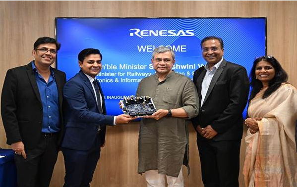
Union Minister for Electronics and IT, Shri Ashwini Vaishnaw, has inaugurated India’s first 3-nanometer (3nm) chip design centres in Noida and Bengaluru, operated by Renesas Electronics India Private Limited. This milestone positions India at the forefront of advanced semiconductor design, marking a significant leap from previous 7nm and 5nm technologies.
The 3nm chips, known for their high transistor density—up to 250 million per square nanometre—offer enhanced performance and energy efficiency. These advancements are crucial for next-generation devices, including smartphones, laptops, servers, and medical equipment.
This initiative is part of India’s comprehensive semiconductor strategy, which encompasses design, fabrication, assembly, testing, and packaging (ATMP), as well as the development of a robust supply chain. The government is also investing in talent development through semiconductor learning kits and Electronic Design Automation (EDA) tools provided to over 270 academic institutions.
Renesas Electronics’ CEO, Hidetoshi Shibata, emphasized India’s strategic importance in the global semiconductor landscape, highlighting the country’s growing contributions in embedded systems, software, and system innovation.
This development signifies India’s commitment to becoming a self-reliant, global hub for semiconductor innovation and manufacturing.